
Scanning electron microscopy (SEM) & EDX analysis –
High-resolution material analysis at the nanometre scale
Failure analysis - material characterization and quality control
Scanning electron microscopy (SEM) enables extremely high-resolution images of surfaces, microstructures and fracture mechanisms. In combination with energy-dispersive X-ray spectroscopy (EDX), chemical elements from atomic number 5/6 can also be reliably determined. SEM /EDX analysis thus provides decisive information for quality assurance, damage analysis, material development and process optimization. As a DIN EN ISO/IEC 17025 accredited testing laboratory, encontec offers independent, reproducible and industry-oriented analyses for mechanical engineering, medical technology, the food industry, electronics, automotive and many other sectors.
Our services:
- High-resolution SEM imaging
- EDX element analysis (point, line, area)
- Fractography & damage analysis
- Analysis of cracks, pores, inclusions, particles
- Layer and cross-sectional examinations
- CL analytics for ceramics, semiconductors, minerals
Your advantage: Accredited, reproducible and industry-oriented material analyses - fast, precise and reliable.
Request SEM/EDX analysis now -
We deliver results you can rely on.
SEM & EDX analysis -
High-resolution material analysis in the nanometer range
In the encontec test laboratory, we examine surfaces, microstructures and fracture mechanisms using state-of-the-art scanning electron microscopy (SEM) and precise EDX element analysis. Our analyses provide clear, reliable results for quality assurance, damage analysis and material development.
Areas of application for SEM and EDX analysis
Materials science
- High-resolution examination of surfaces, fracture surfaces and cross-sections
- Analysis of microstructures, microstructures and material transitions
- Evaluation of layers, coatings and particles
Damage analysis
- Identification of causes of damage using SEM + EDX
- Chemical analysis of inclusions, particles, corrosion residues
- Fractographic evaluation for the reconstruction of fracture mechanisms
Cathodoluminescence (CL detector)
- Analysis of luminescent properties under electron bombardment
- Visualization of defects, zoning, phases and crystal growth
- Ideal for ceramics, semiconductors, minerals, glasses and functional materials
Your advantages at a glance
Highest resolution
Representation of the finest structures down to the nanometer range.
Excellent depth of field
Clearly recognizable details even at very high magnifications.
Maximum variety of materials
Analysis of almost all materials: metals, ceramics, plastics (inorganic components), glass, powders, particles, adhesions and more.
Our SEM and EDX technologies
Scanning electron microscopy (SEM)
- Scanning the surface with a focused electron beam
- Vivid, high-resolution images
- Representation of micro- and nanostructures
Detectors at a glance
SE detector (secondary electrons)
- High-resolution topography
- Ideal for morphology, roughness, fine structures
BSD detector (backscattered electrons)
- Contrast by element weight
- Optimal for material distribution and phase analysis
CL detector (cathodoluminescence)
- Visualization of defects, zoning, crystal growth
- Supplements REM/EDX with electronic and structural information
EDX analytics
- Element determination from boron or carbon
- Point, line and area analyses (spots, linescans, mappings)
- Qualitative and quantitative composition analysis
Typical areas of application
- Fracture surface investigations & fractography
- Analysis of surface topography, roughness and morphology
- Detection of microdefects: Cracks, pores, inclusions
- Phase and material distribution analyses
- Characterization of layers and coatings
- Layer thickness measurements & cross-section analyses
- Powder and particle analysis (incl. nano-powder)
- Chemical analysis of impurities, corrosion products, residues
- Defect and inhomogeneity analyses in functional materials
- Investigation of crystal growth, zoning and stresses
Why encontec?
Accredited test laboratory
Certified quality according to DIN EN ISO/IEC 17025.
Experienced materials laboratory team
Many years of expertise in SEM and EDX analysis - from routine tests to complex damage cases.
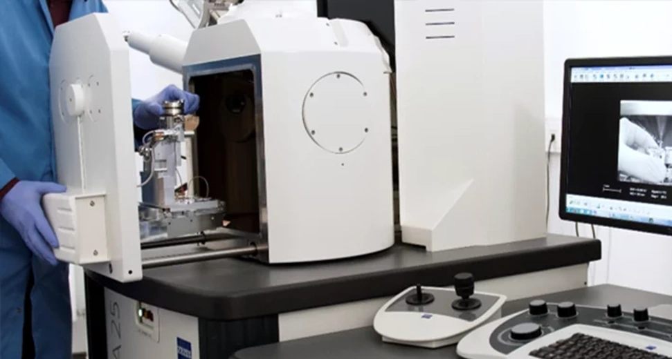
Modern equipment
- ZEISS EVO MA 25
- SE, BSE and CL detectors
- Bruker XFlash EDX system
Industry-related analyses
For product optimization, damage analysis and quality control.
encontec -
Your partner for high-resolution SEM and EDX analysis
Precise, reproducible and metrologically reliable - for safe technical decisions.