Scanning electron microscopy (SEM)
High-resolution material analysis at the nanometre scale
Scanning Electron Microscopy (SEM) Testing Laboratory
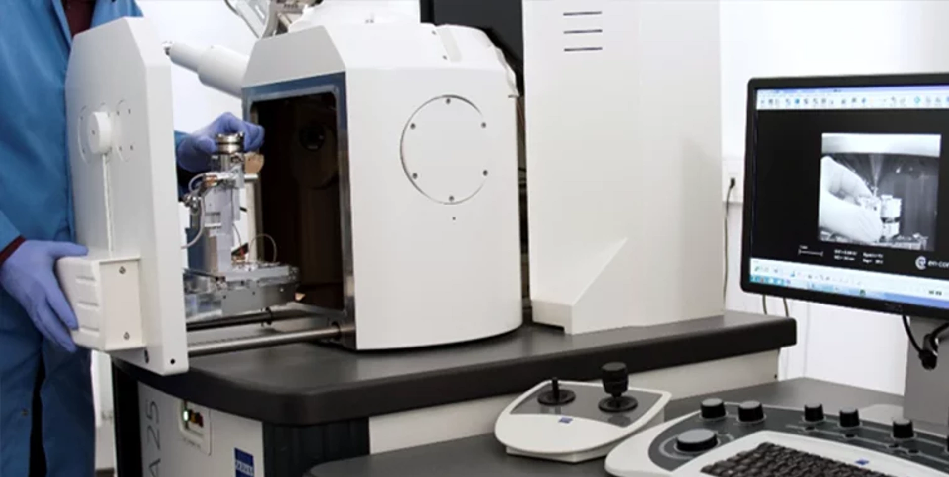
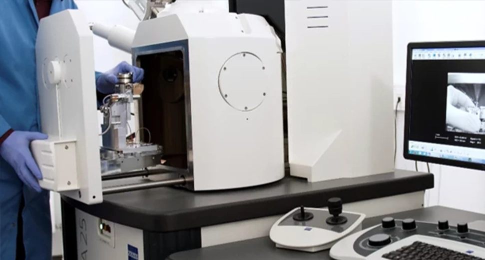
Using scanning electron microscopy, we analyze surfaces, microstructures, and particles in the submicrometer range. The SEM provides high-resolution, three-dimensional images and enables detailed examination of cracks, layer systems, corrosion phenomena, particles, and microstructures. When combined with EDX, you receive precise information about morphology and chemical composition. The CL detector can be used to identify fluorescent plastic layers or cracks. Fluorescent minerals can also be examined.
BENEFITS OF SEM
- Highest resolution: Depiction of the finest structures down to the nanometer range. High-resolution images with a three-dimensional appearance.
- Excellent depth of field: Clearly visible details even at very high magnifications.
- Maximum material diversity: Analysis of virtually all materials: metals, ceramics, plastics (inorganic components), glass, powders, particles, deposits, and more.
Typical use cases:
- Analysis of Cracks, Fracture Surfaces, and Delaminations
- Analysis of Particles, Contaminants, and Foreign Materials
- Evaluation of Layered Structures, Interfaces, and Surface Structures
- Characterization of Corrosion, Wear, and Material Changes
- Support for damage analyses and quality assessments
Scope of Services:
- High-resolution SEM imaging in the sub-micrometer range
- Imaging of Surfaces, Microstructures, and Particles
- Combination with EDX elemental analysis, comparative images, and reference analyses
- Documentation of all relevant findings
Result:
- High-resolution SEM images with clear visualization of microstructures
- Identification of defects, particles, or material deviations
- Comprehensive Documentation of Findings
- Recommendations for Development, Manufacturing, or Failure Analysis
An overview of the detectors in our SEM:
SE detector (secondary electrons)
- High-resolution topography
- Ideal for morphology, roughness, fine structures
BSD detector (backscattered electrons)
- Contrast by element weight
- Optimal for material distribution and phase analysis
CL detector (cathodoluminescence)
- Visualization of defects, zoning, crystal growth
- Supplements SEM/EDX with electronic and structural information